- 您现在的位置:买卖IC网 > Sheet目录1993 > DS1394U-33+T&R (Maxim Integrated Products)IC RTC SPI 3WIRE W/CHRGR 10-MSOP
DS1390–DS1394
Low-Voltage SPI/3-Wire RTCs with
Trickle Charger
19
Maxim Integrated
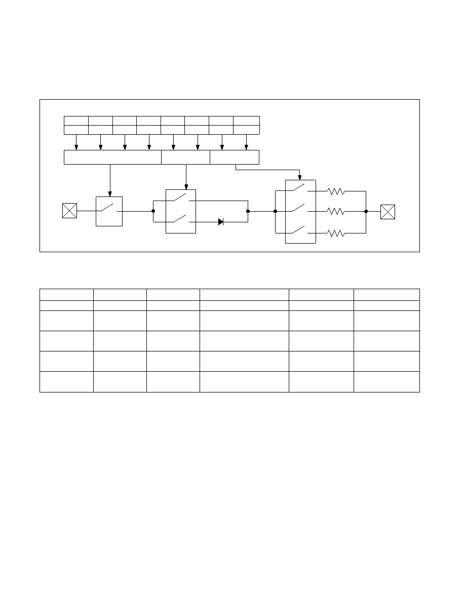
The user determines diode and resistor selection
according to the maximum current desired for battery
or super cap charging. The maximum charging current
can be calculated as illustrated in the following exam-
ple. Assume that a system power supply of 3.3V is
applied to VCC and a super cap is connected to
VBACKUP. Also, assume that the trickle charger has
been enabled with a diode and resistor R2 between
VCC and VBACKUP. The maximum current IMAX would
therefore be calculated as follows:
IMAX = (3.3V - diode drop) / R2
≈ (3.3V - 0.7V) /
2k
≈ 1.3mA
As the super cap changes, the voltage drop between
VCC and VBACKUP decreases and therefore the charge
current decreases.
R1
250
R2
2k
R3
4k
VCC
VBACKUP
BIT 7
BIT 6
BIT 5
BIT 4
BIT 3
BIT 2
BIT 1
BIT 0
TCS3
TCS2
TCS1
TCS0
DS1
DS0
ROUT1
ROUT0
TRICKLE-CHARGE REGISTER (8Fh WRITE, 0Fh READ)
1 0F 16 SELECT
NOTE: ONLY 1010b ENABLES CHARGER
1 OF 2
SELECT
1 OF 3
SELECT
TCS[3:0] = TRICKLE-CHARGE SELECT
DS[1:0] = DIODE SELECT
ROUT[1:0] = RESISTOR SELECT
Figure 8. DS1390–DS1394 Programmable Trickle Charger
MODE
CPHA
CS
SCLK
SDI
SDO
Disable
X
High
Input Disabled
High-Z
Write
0
Low
CPOL* = 0, SCLK Rising;
CPOL = 1, SCLK Falling
Data Bit Latch
High-Z
Read
0
Low
CPOL = 0, SCLK Falling;
CPOL = 1, SCLK Rising
X
Next Data Bit Shift**
Write
1
Low
CPOL* = 1, SCLK Rising;
CPOL = 0, SCLK Falling
Data Bit Latch
High-Z
Read
1
Low
CPOL = 1, SCLK Falling;
CPOL = 0, SCLK Rising
X
Next Data Bit Shift**
Table 6. SPI Pin Function
*
CPOL is the clock-polarity bit set in the control register of the host microprocessor.
**
SDO remains at high-Z until 8 bits of data are ready to be shifted out during a read.
发布紧急采购,3分钟左右您将得到回复。
相关PDF资料
DS14285SN+T&R
IC RTC W/NV RAM CNTRL 24-SOIC
DS1486P-120+
IC TIMEKEEPER RAM 1MB 34-PCM
DS1500WE
IC RTC Y2KC W/NV CTRL 32-TSOP
DS1501YSN+T&R
IC RTC WDOG Y2K 5V IND 28-SOIC
DS1553P-70+
IC RTC RAM Y2K 5V 70NS 34-PCM
DS1554W-120IND
IC RTC RAM Y2K 3.3V 120NS 32EDIP
DS1556WP-120IND
IC RTC RAM Y2K 3.3V 120NS 34PCM
DS1557P-70IND
IC RTC RAM Y2K 5V 70NS 34PCM
相关代理商/技术参数
DS1395
制造商:DALLAS 制造商全称:Dallas Semiconductor 功能描述:RAMified Real Time Clock
DS1395N
制造商:未知厂家 制造商全称:未知厂家 功能描述:Peripheral IC
DS1395S
制造商:DALLAS 制造商全称:Dallas Semiconductor 功能描述:RAMified Real Time Clock
DS1395SN
制造商:未知厂家 制造商全称:未知厂家 功能描述:Peripheral IC
DS1397
制造商:DALLAS 制造商全称:Dallas Semiconductor 功能描述:RAMified Real Time Clock
DS-14
功能描述:非热缩管和套管 FLEX BRAIDED SHIELD 14MM X 100M ROLL
RoHS:否 制造商:Panduit 产品:Cable Wraps 类型:Spiral 颜色:Black 材料:PP 内径:0.03 in 长度:100 ft
DS14-00
制造商:FLOWLINE 功能描述:Sensor, Liquid Level, Ultrasonic Switch/Control 4 Relays; Range 49.2 in, 1NPT
DS1-40-0001
制造商:SCHURTER 制造商全称:Schurter Inc. 功能描述:Storage Choke, fully potted resign